Designing a chip with TinyTapeout
I have always wanted to fully understand the process of designing and manufacturing computer chips. This weekend I dipped my feet in the water with the TinyTapeout project.
First some context. Efabless as part of their Open Shuttle Program, sponsored by Google and Skywater, is trying to encourage innovation in chip design and manufacture. They allow anyone who is okay with open sourcing their complete circuit design to submit a design, which is subsequently manufactured by Skywater. This is pretty cool as it allows students, hobbyist, and perhaps very small commercial entities to test their designs for a very cheap price of 10k USD.
Now, the chip size provided by Efabless is pretty large (about 10 sq nm) and still quite expensive for students, so the people at TinyTapeout had a brilliant idea. Let many students submit about 500 different designs for very simple circuits (about 200 gates at the maximum), and these will then be put on a single chip. Each person intending to get a chip only pays about 25 USD, which is within reach of a lot more people.
My submission is an educational implementation of the [7,4,3] Hamming error-correcting code. Here 4 bits are encoded into 7 bits such that the any single-bit error can be corrected. It's a very simple code, where the 4 data bits are copied as is. The last 3 bits store the parities of various combinations of these bits. , and , where the addition is done without carrying. The wikipedia article explain very well why an error on any single bit can be corrected easily, but one can figure this out quite easily by noting which parities are disturbed for an error on each bit.
The main constraint on the design was that I only had 8 toggles to determine the input and 8 outputs. Hence, I provided the following functionality.
- The user can determine the 4 data bits. This obviously consumed 4 of the input toggles.
- The user can choose which one, if any, of the 7 encoded bits gets a bit-flip error. This consumed 3 toggles. If these 3 toggles were all off, then no error was introduced. If some were on, then 3 bits converted to binary determine the index of the flipped bit.
- The final toggle to decide if decoding is applied or not to correct the error.
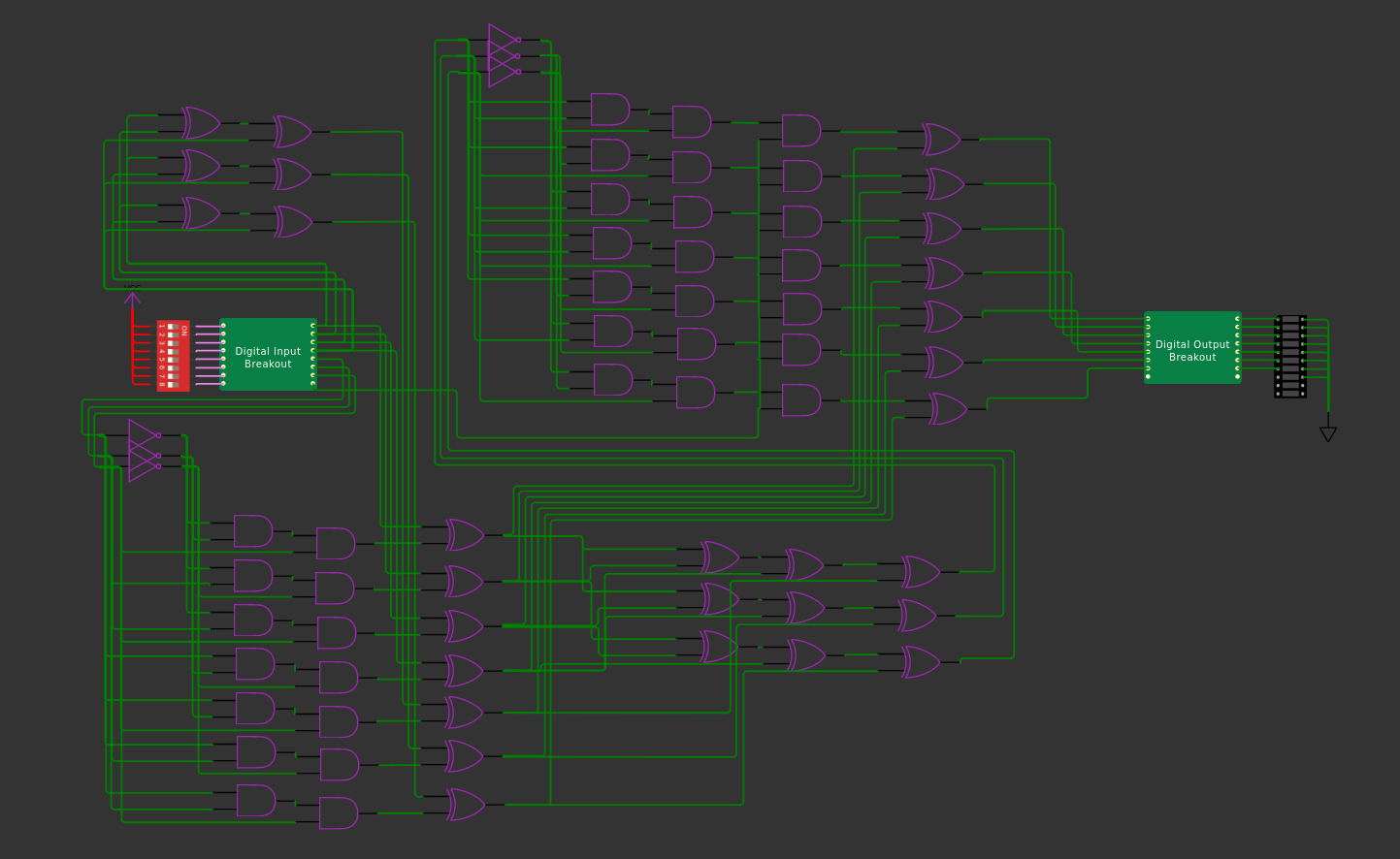
I designed the entire circuit myself, and it is shown below.

As you will note, it is entirely made of XORs, ANDs and NOTs. XORs are great because they can be used to sum two bits as well as compare two bits, both of which are required over and over again. The top left of the circuit is the encoding process. I use a sequence of XORs to compute the 3 parity bits, as we are just adding bits.
The bottom left of the circuit is where the user selected error is applied. Here we have to use the 3 bits to decide which wire gets flipped. Here, I use a simple trick that I personally learned in quantum computing. Think of the 7th bit, which should be flipped if the user-toggles are 111. This can be done by passing the user-input through two AND gates.

Note that the output is 1 only if all three inputs are 1. We can add the output of this piece to the 7th encoded bit using a XOR, and only if the user-toggle is 1 will the 7th bit be flipped.
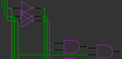
What about the other possibilities. We simply use NOTs to create the correct controlled operation. The first wire triggers on 001. So if we first flip the two input bits and then pass then through the ANDs, then only 001 will result in the correct output, which can be seen below.

The other possibilities can be done in similar fashion.
For decoding, we need to recompute all parities and compare them with the existing parity bits. This is done in the bottom right. We get three bits again which has information on which bit is flipped. We use this to re-flip it using the same idea of NOTs and ANDs to create controlled-operations in the top right. The only difference is that before flipping, we use the 8th toggle and AND gates to determine if the bit should be flipped or not.
This was a pretty fun exercise, and I had a mix of pleasure and pain putting the design into the software provided while keeping it legible.
Finally, I submitted the design, and it was converted into what will be implemented on the actual chip. This is the image spit out by the compiler, though I don't know how to read it at all.
My project lives in a github repository. Take a look if you are interested.